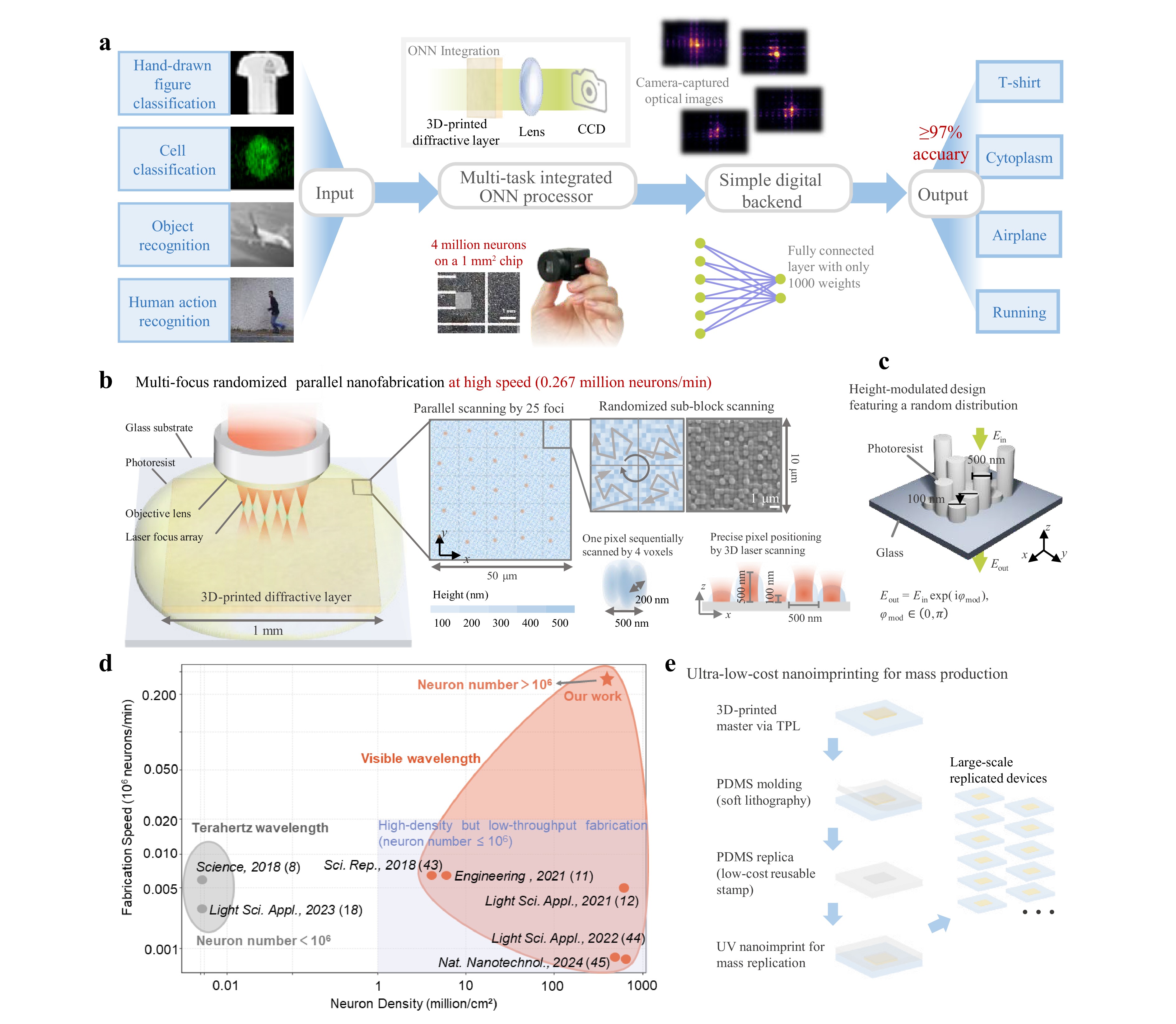

GA, UNITED STATES, July 17, 2026 /EINPresswire.com/ -- Energy-efficient visible-band intelligent vision processors demands both optical neural network (ONN) design and high-speed nanofabrication advances. Chinese researchers proposed a random-projection ONN design strategy and established a multi-focus random-access nanofabrication platform that fabricates visible-light ONN devices with 4 million optical neurons per mm² in just 15 minutes, hitting a new record. Miniaturized camera integration ensures high-accuracy complex vision tasks with low power consumption, advancing optical sensing, medical diagnosis and human-computer interaction.
The rapid advancement of deep learning has revolutionized machine vision, yet traditional von Neumann hardware struggles with the speed and power demands of processing high-resolution data. Optical neural networks (ONNs) provide a promising alternative by performing computations at the speed of light with minimal energy. However, implementing ONNs at visible wavelengths requires millions of wavelength-scale neurons, presenting immense fabrication challenges for traditional methods.
In a new paper published in Light: Advanced Manufacturing, a team of scientists, led by Professor Shih-Chi Chen and Professor Chaoran Huang from The Chinese University of Hong Kong, introduced a breakthrough high-throughput randomized multi-focus two-photon lithography (TPL) platform. By employing a novel parallel scanning strategy via holographic light-field control, the team successfully fabricated four million 500-nm neurons on a millimeter-scale chip in just 15 minutes.
This work utilizes a task-agnostic optical encoder that performs random projections through a 3D-printed diffractive layer. The system integrates this optical device and a compact camera with a simple digital neural network readout layer parameterized by as few as 1,000 weights. Experimental results demonstrate superior performance with 97%—99% classification accuracy in diverse tasks, including hand-drawn figure recognition, human action recognition, and human face keypoint detection.
Unlike conventional lithography, which is time-consuming and costly, this multi-focus TPL approach supports rapid prototyping and is compatible with ultra-low-cost UV nanoimprinting for mass production. This capability bridges the gap between high-precision prototyping and scalable manufacturing, paving the way for the broad deployment of integrated optical vision processors in applications such as LiDAR, biomedical diagnostics, and human-computer interaction.
These scientists highlight the versatility of their technique: "Since the diffractive layer implements an untrained random projection, it serves as a task-agnostic optical encoder, while task adaptation is achieved exclusively through retraining of the lightweight digital readout layer."
Regarding scalability, the scientists noted: "Unlike conventional metasurfaces or other optical neural network platforms, which typically rely on one-off or costly fabrication schemes and thus face significant barriers to scalability, our method intrinsically supports cost-effective mass production. This unique capability bridges the gap between high-precision prototyping and scalable device manufacturing, thereby offering a practical and economical pathway towards the deployment of optical neural networks."
Looking ahead, the team forecasts: "With broader material selection and nanoimprint replication strategies, the operational range could potentially extend from the near-UV to infrared regimes. In addition, centimeter-scale devices are feasible through tiled writing and imprint replication, enabling larger optical apertures for practical imaging systems."
References
DOI
Original Source URL
https://doi.org/10.37188/lam.2026.096
Funding information
This work was supported by the HKSAR Research Grants Council, Research Grant Council (RGC) YCRG C4004-24Y, C1002-22Y, ECS 24203724, 14211224, C4074-22GF, T46-705/23-R, SRFS2526-4S01; Innovation and Technology Commission (ITC) ITS/237/22; InnoHK Centre projects funded by the Innovation and Technology Commission A-CUHK-16-5-14; NSFC 62405258; Basic Research Program of Jiangsu (No.BK20253062); Fundamental Research Funds for the Central Universities (No.30925010603); and National Key Laboratory of Integrated Circuits and Microsystems (No: NICL2025KF2001).
Lucy Wang
BioDesign Research
Legal Disclaimer:
EIN Presswire provides this news content "as is" without warranty of any kind. We do not accept any responsibility or liability for the accuracy, content, images, videos, licenses, completeness, legality, or reliability of the information contained in this article. If you have any complaints or copyright issues related to this article, kindly contact the author above.

Media gallery